Overview
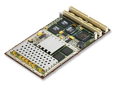
The ICS-8554B uses four 14-bit ADCs (Texas Instruments ADS5424), which sample synchronously at frequencies of up to 105 MHz using either a fixed frequency onboard oscillator or an external frequency source. Clock, trigger, and sync sources are all selected by software control. The user is not required to move any jumpers or wire links. Clock input may be sinusoidal or LVTTL. The inputs to the converters are transformer coupled. The outputs of the two ADCs are passed to a Xilinx Virtex-II FPGA (XC2V3000).
Abaco Systems maintains a library of FPGA cores such as wideband DDC, FFT, and demodulation functions - (contact the factory for details). From there the ADC data can be written directly into the FIFO memories, or routed through the GrayChip GC4016 ASICs for digital down conversion. Data may be moved to host processors either over the PCI 2.2 64/66 interface, or over the user defined Pn4 connection. The Pn4 connection may be used as a digital data input port, to accept data from other cards. Both these interfaces are capabale of sustaining aggregate (not burst) bandwidths in excess of 400 MBytes/sec.
The ICS-8554B is available in five ruggedization levels conforming to the IEEE 1101.2-1992 standard, including both convection- and conduction-cooled options, and can be used with any suitable type of carrier card that will accept a PMC module, including VME, PCI and CompactPCI types. Level 4 and 5 conduction-cooled versions must be used with an appropriate conduction cooled carrier such as those made by Abaco Systems in VMEbus and CompactPCI formats.
- 4 ADC channels
- 14-bits @ 105 MHz
- 2 GrayChip GC4016 DDC ASICs
- 3M gate Xilinx Virtex-II FPGA
- 2 MBytes of FIFO storage
- Pn4 user I/O supports LVTTL or LVDS signalling levels
- Windows, Linux and VxWorks device drivers
- Extensive application and technical support available
- Sensor Processing Resource Center
- Ruggedization Levels
Specifications
Downloads

White Papers
Solutions Briefs

Notices
Request A Quote
ICS-8554B

Contact An Expert
Looking for help with ICS-8554B

Get Support
Looking for help with ICS-8554B


