Overview
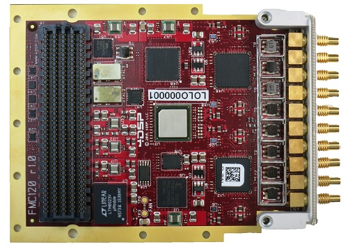
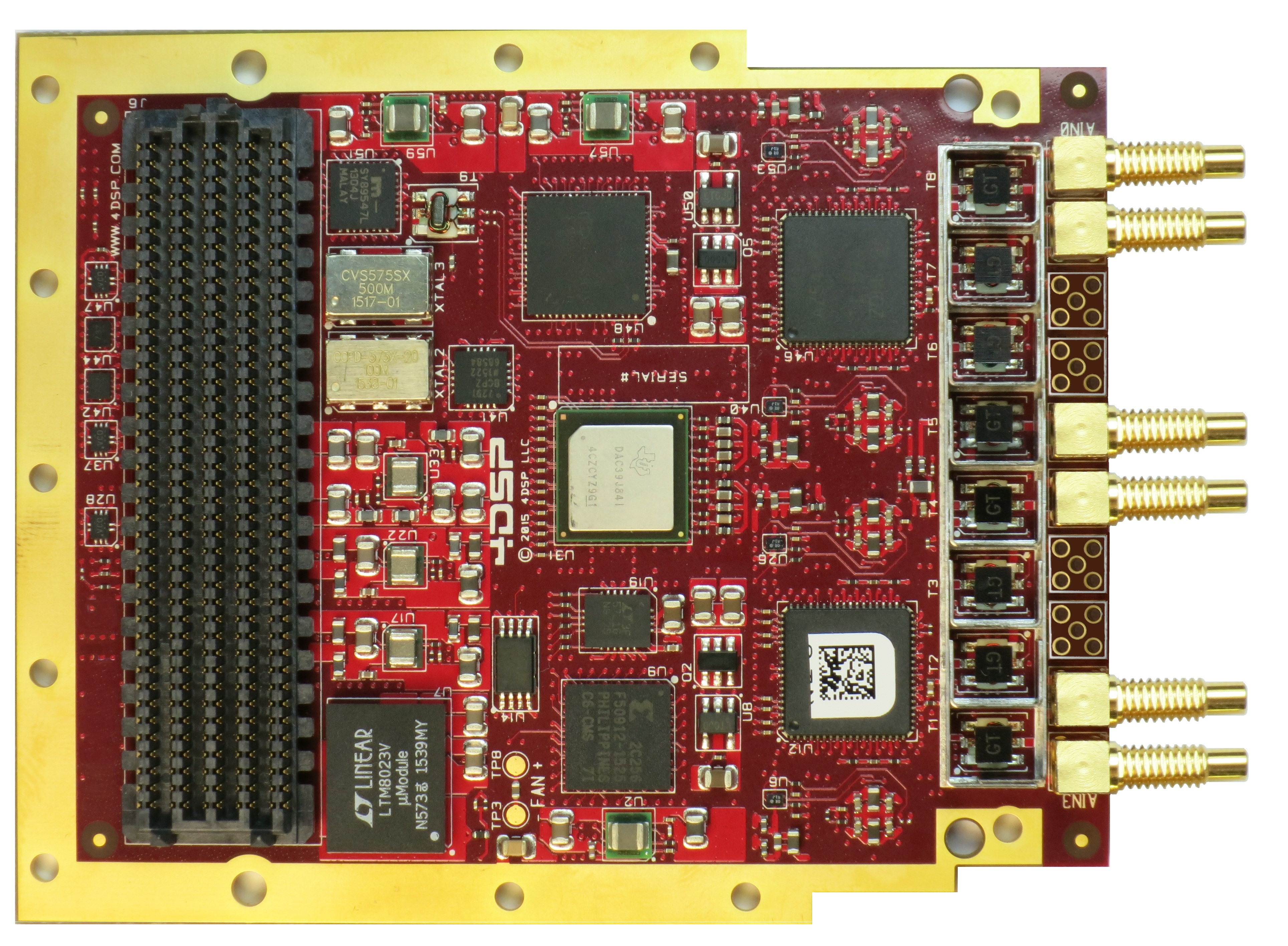
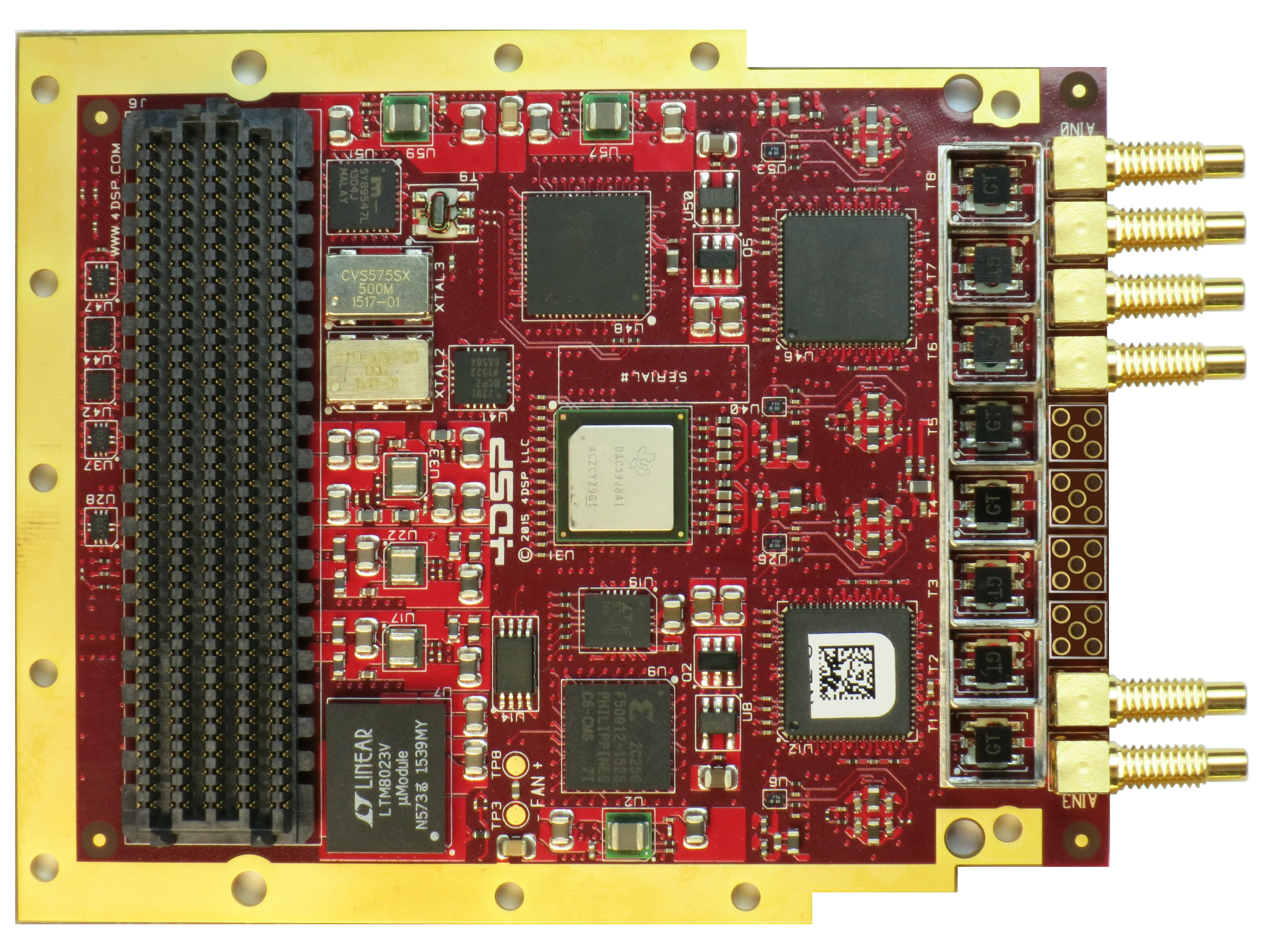
The FMC120 provides four 16-bit A/D channels up to 1Gsps, four16-bit D/A channels up to 1.25Gsps and up to 2.8Gsps sample rate with interpolation. The devices can function up to 1Gsps during simultaneously D/A and A/D operation as the clock source is shared.
The design is based on Texas Instruments' ADS54J60 Analog-to-Digital converter and Texas Instruments' DAC39J84 Digital-to-Analog converter.
The sample clock can be supplied externally through a coax connection or supplied by an internal clock source (optionally locked to an external reference). Additionally, a trigger input is available for customized synchronization.
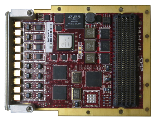
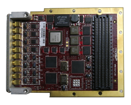
The FMC120 is mechanically and electrically compliant to the FMC standard (ANSI/VITA 57.1). The card connects to an FPGA carrier card through a standard high-pin count (HPC) connector. Front panel I/O can optionally be populated with MMCX or SSMC coaxial connectors.
Analog I/O is DC coupled.
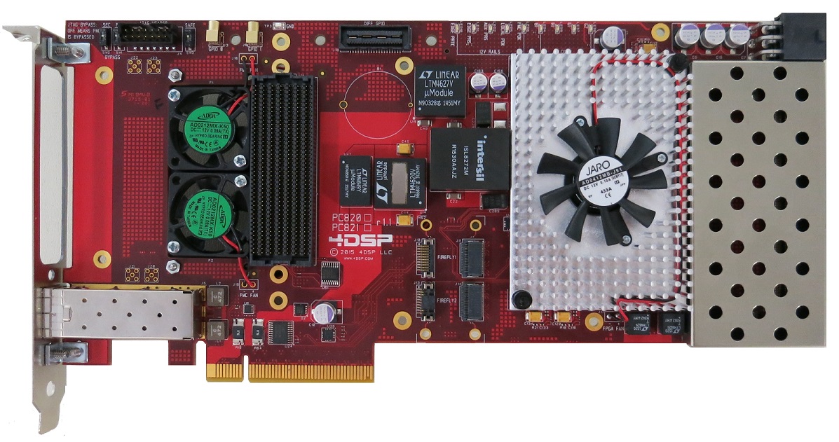
The FMC120 is designed to be used in convection- or conduction cooled environments. When paired with the latest FPGA carrier cards such as the 4DSP VP868 with Xilinx Ultrascale technology, customers can innovate high performance algorithms on an industry standard platform.
Board Support Package
Our Board Support Package helps customers get their hardware implementation underway as quickly as possible by providing reference designs, the Stellar IP FPGA development tool, and the 4FM GUI user interface for controlling and monitoring the hardware, as well as other supporting elements.

FMC.gif
Specifications
Downloads

Datasheets
Solutions Briefs

Manuals

White Papers
Request A Quote
FMC120 FPGA Mezzanine Card

Contact An Expert
Looking for help with FMC120 FPGA Mezzanine Card

Get Support
Looking for help with FMC120 FPGA Mezzanine Card
