Overview
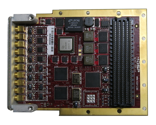
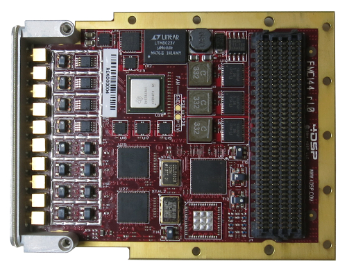
The FMC142 is an analog-to-digital (A/D) and digital-to-analog (D/A) FMC daughter card that provides two 16-bit A/D channels at 370 MSPS and two 16-bit D/A channels at 2.5 GSPS which can be clocked by an internal clock source (optionally locked to an external reference) or by an externally-supplied sample clock. A trigger input is also available for customized sampling control.
It is mechanically and electrically compliant with the FMC standard (ANSI/VITA 57.1-2010), offers front panel analog I/O access and can be used in a conduction-cooled environment.
The design is based on Texas Instruments' ADC16DX370 dual-channel 16-bit 370MSPS ADC and DAC38J84 quad-channel 16-bit 2.5 GSPS DAC.
The analog signal inputs are either AC or DC-coupled and connected to MMCX/SSMC coax connectors on the front panel.
The FMC142 allows flexible control of sampling frequency and offset correction through serial communication buses.
The card is equipped with power supply and temperature monitoring and offers several power-down modes to switch off unused functions.
The FMC142 is ideal for applications where limited space is available such as radar/sonar, wireless telecommunications, and aerospace test and measurement instruments.
It also features a JESD204B serial interface to provide a simplified high-speed interface between the data converters and the FPGA with a minimum of digital I/O on the board. The module therefore delivers high-bandwidth connectivity suited for a wide range of calculation-heavy FPGA-based applications such as beamforming, direction finding, and software-defined radio (SDR).
Board Support Package
Our Board Support Package helps customers get their hardware implementation underway as quickly as possible by providing reference designs, the Stellar IP FPGA development tool, and the 4FM GUI user interface for controlling and monitoring the hardware, as well as other supporting elements.

FMC.gif
Specifications
Downloads

Datasheets
Solutions Briefs

Manuals

White Papers
Request A Quote
FMC142 FPGA Mezzanine Card

Get Support
Looking for help with FMC142 FPGA Mezzanine Card


