Overview
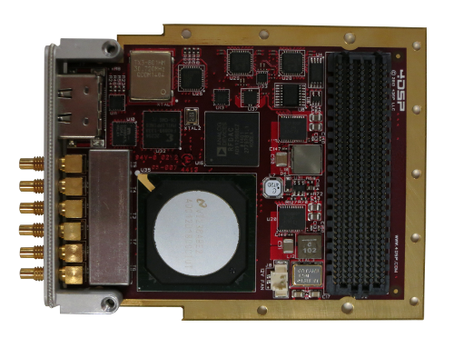
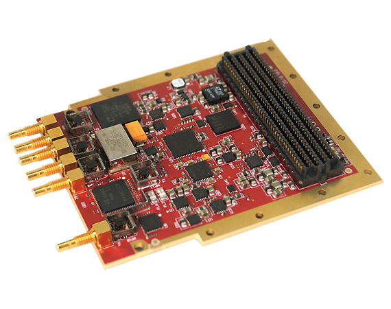
The FMC160 provides one 12-bit A/D channel at 3.6Gsps and one 14-bit D/A channel at 5.7Gsps (2.85Gsps direct RF synthesis) clocked by either an internal clock source (optionally locked to an external reference) or an externally supplied sample clock. In addition, a trigger input for customized sampling control is available to users. It is mechanically and electrically compliant with the FMC standard (ANSI/VITA 57.1).
With a high-pin count connector, front panel I/O, and able to be used in a conduction cooled environment, the design is based on Texas Instruments' ADC12D1800 Analog-to-Digital converter and Analog Devices' AD9129 Digital-to-Analog converter. The analog signals are AC-coupled, connecting to MMCX or SSMC coax connectors on the front panel.
The FMC160 allows flexible control on clock source through serial communication buses.
Furthermore, the card is equipped with power supply and temperature monitoring and offers several power-down modes to switch off unused functions in order to reduce system-level power consumption. It is well suited for low power applications such as airborne where the highest level of performance is required while ensuring that mission range is not affected.
Board Support Package
Our Board Support Package helps customers get their hardware implementation underway as quickly as possible by providing reference designs, the Stellar IP FPGA development tool, and the 4FM GUI user interface for controlling and monitoring the hardware, as well as other supporting elements.

FMC.gif
Specifications
Downloads
Solutions Briefs

Manuals

White Papers
Request A Quote
FMC160 FPGA Mezzanine Card

Contact An Expert
Looking for help with FMC160 FPGA Mezzanine Card

Get Support
Looking for help with FMC160 FPGA Mezzanine Card


